One of the most misunderstood ratings for transient voltage suppressor (TVS) diodes is peak pulse power (PPP). Many engineers will select surge protection components based primarily on rated peak pulse power and assume that their system will be well protected. After all, it seems logical to assume that a higher power rating means the device can absorb higher transient currents and therefore should be superior. While peak pulse power ratings may be considered in the selection process, the device should not be chosen solely on this parameter. To illustrate why, let us review the definition of TVS peak pulse power.

What is TVS Peak Pulse Power?
The peak pulse power rating of a TVS diode is defined as the instantaneous power dissipated by a device for a given pulse condition, and is a measure of the power that is dissipated in the TVS junction during a given transient event. It is calculated by the following relationship: PPP = VC x IPP, where PPP = Peak Pulse Power (W), VC = Clamping Voltage (V) and IPP = Peak Pulse Current (A). Let us examine what each of these parameters means.
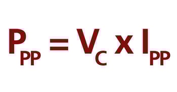
Figure 1: Peak Pulse Power Calculation

TVS diodes are connected in parallel with the protected IC (Figure 2). Under normal operating conditions, the TVS diode presents a high impedance to the protected circuit. During an electrical over-stress (EOS) event, once the voltage surpasses the TVS breakdown voltage, the device “turns on” and becomes a low impedance path to shunt the transient current to ground. This current is defined as the “peak pulse current.” The voltage developed across the device at a specified peak pulse current is the clamping voltage. The clamping voltage must be lower than the failure voltage of the protected IC. TVS manufacturers go to great lengths to develop technology for lowering TVS clamping voltage while maintaining high peak pulse current handling capabilities.
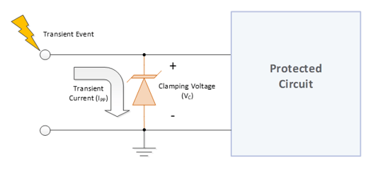
Figure 2: TVS Diode Connection
Before going further, it is important to have a good understanding of how the peak pulse current waveform is specified. Under transient conditions, TVS diodes dissipate power in the junction of the device. TVS junctions are designed to handle high transient energy for a given junction size. We defined PPP as the product of IPP and VC for a given pulse or pulse width. This is an indirect way of quantifying the energy handling capability of the device since energy is power multiplied by time. In this case, the time is given by the pulse duration. The majority of TVS diode IPP and PPP ratings are defined using industry standard double exponential waveforms, most commonly called out in IEC 61000-4-5. The IEC 61000-4-5 standard current waveform is a double exponential with an 8µS rise time and a 20µs decay, or 8/20µs as shown in Figure 3.
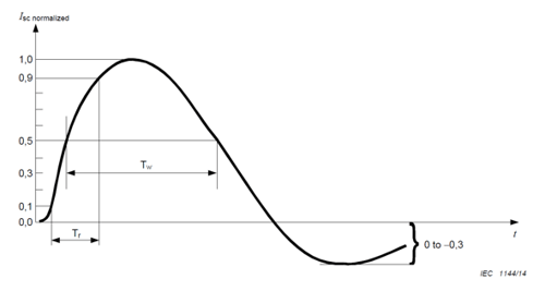
Figure 3: Double Exponential Waveform (Taken from IEC Standard: Electromagnetic compatibility (EMC) – Part 4-5: Testing and measurement techniques – Surge immunity test, IEC 61000-4-5, 2014)
Looking at a practical example, consider the peak pulse current versus clamping voltage IV characteristic plots shown in Figure 4. In this example, three options for selecting a TVS diode (TVS 1, TVS 2 and TVS 3) are considered. The IC to be protected has a failure voltage of 14V and the application requires a surge test current of 10A per IEC61000-4-5. This means that in order to protect the IC, the TVS should have a clamping voltage below 14V for peak pulse currents of 10A and above. Each TVS device has the same breakdown voltage of approximately 7V, and are rated for maximum peak pulse current of 20A per IEC 61000-4-5. The PPP rating of TVS 1 is 300W for a 20A pulse (PPP = 20A * 15V), the PPP rating of TVS 2 is 400W for a 20A pulse (PPP = 20A * 20V), and finally the PPP rating of TVS 3 is 500W for a 20A pulse (PPP = 20A * 25V). TVS 1 is designed with lower clamping characteristics and does not reach the IC failure voltage of 14V until the device is conducting an IPP of 17A, well above the 10A requirement. TVS 2 does not reach the 14V clamping until just under 11A. Theoretically, this device would protect the IC, however there is very little design margin. TVS 3 clamps at 14V at an IPP of approximately 7A. In other words, due to the higher clamping characteristic, a 10A pulse will likely damage the IC even though the TVS will remain undamaged. In this scenario, TVS 1 (300W) is the best solution, despite the lower peak pulse power rating when compared to TVS 2 (400W) and TVS 3 (500W).
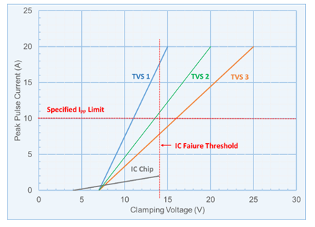
Figure 4: IV Clamping Characteristic Curves
The above example illustrates the point that with all other factors accounted for, lower clamping voltage will translate to a lower PPP rating, but a higher level of protection. Therefore, in reality, the peak pulse power rating is a measure of how much power the TVS can absorb without damage, but does not predict how well the TVS will protect the sensitive circuit. It is more important to focus on clamping voltage for a given current as a measure of how well the TVS will protect your circuit.
Learn more about Semtech’s leading TVS diodes, as well as other applications from its diverse circuit protection product portfolio, on the Semtech website.

Semtech and the Semtech logo are registered trademarks or service marks of Semtech Corporation or its affiliates.