Picture bustling factories filled not with massive, outdated machines but with streamlined, efficient counterparts: robots darting around, intricate sensors overseeing every process, and data seamlessly flowing for real-time control. To tackle the challenges posed by critical industrial environments, engineers actively seek integrated circuits (ICs) housed in semiconductor packages known for their resilience and reliability. These packages must demonstrate exceptional thermal and mechanical durability and robust electrical performance under demanding conditions, ensuring optimal functionality and prolonged system life.
In response to the demands of modern industry needs, the semiconductor industry has introduced leadless surface-mount device (SMD) packages for ICs, which enable the integration of a vast number of electronic components within a circuit. The era of bulky electronics in industrial applications is fading as advanced technology enables denser circuits in more confined spaces, resulting in sleek, lightweight machines capable of operating in tight quarters. As ICs undergo evolution and miniaturization, their corresponding packages also undergo a transformation, becoming increasingly compact. This trend extends to ESD protection devices, such as Transient Voltage Suppression (TVS) diodes, employed to safeguard industrial applications' signal interfaces and power lines.
Within the orbit of PCB assembly, numerous surface-mount IC packages play pivotal roles in enhancing the functionality of electronic devices. The DFN (Dual Flat No-Lead) packages are noteworthy among them, distinguished by their compact dimensions and impressive versatility. In this blog, we will explore the benefits of utilizing DFN packages and their use in TVS diodes for ESD protection of industrial applications.
Background on Semiconductor Packaging Assembly
The magic of semiconductor packaging assembly lies in the intersection of science, engineering, and a touch of artistry. It's about efficiency, reliability, and affordability, transforming tiny chips into the workhorses that power our world, from smartphones to spacecraft.
Semiconductor packaging assembly goes beyond merely enclosing the silicon chip; it involves crafting a micro-environment where the tiny silicon chip can survive and operate at its maximum potential. The design of a standard semiconductor package aims to supply electrical power to the chip and facilitate the distribution of signals to and from the silicon chip. Additionally, it dissipates the heat generated by the IC to maintain it within the permissible temperature range. Not only that, the package shields the chip from various factors, including moisture, electromagnetic radiation, temperature fluctuations, and mechanical vibration. Packaging assembly technologies can be broadly placed in two categories – wire bonding and flip chip technology.
In the wire bond semiconductor packaging assembly shown in Figure 1, the silicon die is affixed to the substrate with its active side facing upwards. Subsequently, delicate wires composed of materials like gold, aluminum, or copper are connected from the bonding pads on the silicon die to the corresponding metal leads or pads on the package.
-1.jpg?width=500&height=250&name=Figure-1%20(1)-1.jpg)
Figure 1. Wire bond technology
In the assembly process of flip-chip packaging, solder bumps replace wire bonds to connect the IC to the substrate. This method involves the deposition of minuscule solder bumps on the chip pads, acting as the interconnection points between the chip and the substrate. Subsequently, the die is inverted, positioning its active side with the solder bumps facing downward. The flip-chip technology is shown in Figure 2. A significant benefit of flip-chip technology lies in its ability to allow vertical stacking of dies atop each other—a task that proves more challenging with wire-bonded chips due to the presence of wires. Flip-chip technology excels in creating dense interconnections within a smaller area with shorter interconnection lengths.
.jpg?width=500&height=250&name=Figure-2%20(1).jpg)
Figure 2. Flip-chip technology
In ESD protection devices, semiconductor packaging assumes a particularly vital role. A TVS diode, for instance, plays a crucial role in enabling the electronic circuit to endure an ESD event by redirecting surges away from the components it safeguards. Since electrostatic spikes during such events can reach tens of thousands of volts, posing a threat to the delicate electronics in modern systems, the active avoidance of possible faults due to such phenomena in assembled finished products demands the use of robust protection measures.
Why Use Leadless DFN Packages for Industrial Applications?
When engineers design industrial applications, they prefer robust and dependable packages capable of withstanding challenging environments and extreme electrical conditions. Until recently, a prevalent choice in industrial applications involved using leaded IC packages. The rationale behind opting for leaded packages is their ease of mounting on PCBs. The leads facilitate swift visual inspection of a PCB, enabling the detection and troubleshooting of broken connections. Additionally, leaded packages are cost-effective and exhibit good heat-dissipating characteristics. However, many leaded packages have significant parasitic effects, constraining their performance in various applications. Furthermore, because of their size, these leaded SMD packages occupy a substantial portion of the PCB.
Over the years, the leadless DFN packages have gained popularity in industrial applications, primarily for these advantages:
-
Compact Dimension and Space-Saving
DFN packages distinguish themselves by the absence of extended leads; their contact points are situated underneath the component rather than along its perimeter, resulting in a more condensed form factor. Consequently, these packages provide noticeable space savings compared to leaded SMD packages. For instance, consider a leaded SOT23 package with dimensions around 2.9mm x 1.6mm, yielding a footprint area of 4.64mm². In contrast, a DFN 1006 package, measuring approximately 1.0mm x 0.6mm, boasts a footprint area of around 0.6mm². This equates to a remarkable 87% reduction in PCB space. The comparison of these two package sizes is shown in Figure 3.
.jpg?width=500&height=250&name=Figure-3%20(2).jpg)
Figure 3. Comparison of package sizes between SOT-23 and DFN 0402 (1006 Metric)
-
Outstanding Thermal Performance
The remarkable heat dissipation capabilities, or thermal performance, of leadless DFN packages, position them as a preferred option for industrial applications. Their clever design incorporates an exposed thermal pad at the bottom, seamlessly bonding with the PCB. This functions as an integrated heat sink for the IC, establishing a direct path for heat to disperse onto the PCB, eliminating the need for an additional bulky heatsink. This design yields a more compact package and facilitates a shorter route for heat dissipation. Moreover, compared to traditional leaded packages, the larger contact area ensures superior thermal efficiency, making DFNs the optimal choice for industrial applications where precise temperature control is crucial.
-
Better Electrical Attributes
DFN packages exhibit lower parasitic inductance and capacitance compared to their leaded SMD counterparts. The presence of these parasitic elements in a leaded SMD package has the potential to constrain the frequency response or compromise the signal integrity of an otherwise resilient circuit design. In contrast, DFN packages excel in signal integrity performance, rendering them particularly appealing for high-speed applications.
-
Mechanical Strength
Another advantage of leadless DFN packages is their ruggedness. The DFN packages are designed with larger contact areas at the bottom of the package and are soldered directly to the PCB. Figure 3 shows the contact area to package ratio of the SOT-23 and DFN 1006 packages. This ensures a reliable contact between the DFN 1006 package and the PCB, where the majority of the package is bonded.
The Challenge and the Solution: Semtech’s DFN Packages with Side-Wettable Flanks
The challenge associated with leadless DFN packages lies in the limited visibility of solder joints on PCBs during the post-package assembly process, as these connections are concealed beneath the package and remain unseen from both the top and sides. Consequently, confirming the proper bonding of the IC to the PCB becomes uncertain. To tackle this challenge, Semtech has introduced TVS diodes in DFN packages that feature a solution called side-wettable flanks.
Side-wettable flanks utilize a technique to ensure that solder spreads from the bottom of the IC, flows up the side of the wall, and forms a visible solder fillet. This feature enables visual examination of the "bumps" formed between the vertical side of the lead and the solder pad on the PCB. Consequently, an automated visual inspection (AVI) system can confirm the adequacy of every electrical joint, validating the proper bonding of ICs to PCBs and ensuring reliable connections (Figure 4). AVI plays a crucial role in scrutinizing the visual appearance of electronic components, assemblies, or PCBs to identify defects, errors, or anomalies in the manufacturing process.
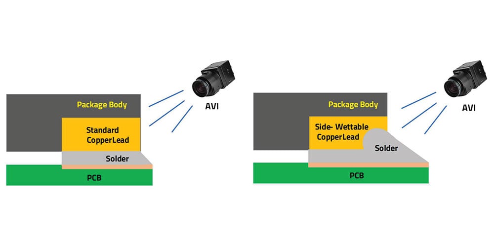
Figure 4. Illustration of the AVI system confirming the correct bonding of a DFN package on a PCB: without a side wettable flank (on the left) and with a side wettable flank (on the right)
Side-wettable flanks offer several additional advantages. They enhance reliability and subsequently improve yield. Semtech’s side-wettable flank technology, illustrated in Figure 5, establishes a robust connection between the IC and the PCB, preventing ICs from separating even in applications subject to vibration or shaking. Simultaneously, this technology contributes to cost and time savings. Tin plating is used to cover the copper terminals as a protective layer, safeguarding the copper from oxidation over time.
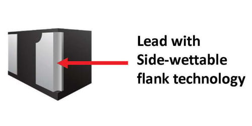
Figure 5. Semtech’s DFN package with side wettable flank technology
TVS Diodes From Semtech Featuring Side-Wettable Flanks
Semtech has introduced a range of single-line TVS diodes, outlined in Table 1, packaged in 0402 size (1.0mm x 0.6 mm x 0.55mm) DFN format utilizing flip-chip technology and featuring side-wettable flanks (SWF) tailored for non-automotive industrial applications. These TVS diodes serve diverse functions, providing ESD protection for Thunderbolt 3, USB 3.0/3.2, USB Type-C connectors on high-speed signal lines, CC/SBU lines, VBus lines, and D+/D- lines. Moreover, they are suitable for safeguarding against ESD in RF & FM Antennas, touchscreen controllers, 12V DC lines, side-keys/keypads, Audio ports, IoT devices, portable instrumentation, general-purpose input-output (GPIO) lines, and, of course, industrial equipment.
|
Part Number |
Number of Lines |
Configuration |
VRWM |
VBR (Min) |
VCLAMP (8/20µs) |
IPP Max (8/20µs) |
RDYN (Typ) |
Cap (Max) |
ESD Rating (IEC) Contact/Air |
Package |


Table 1: Wide range of Semtech parts in DFN packages for protecting industrial applications
Conclusion
Semtech is as a prominent manufacturer of TVS diodes using DFN packages incorporating side-wettable flanks. The DFN package with side-wettable flank technology conserves board space and provides excellent visibility of solder joints for Automated Visual Inspection (AVI), enhancing reliability and yield. Additionally, the DFN package with flip-chip technology also offers superior heat management capabilities and heightened power density. Today’s intelligent industrial applications need TVS diodes in DFN packages with side-wettable flanks to protect power lines, communication buses, and interfaces adequately. Visit Semtech.com to know more.
Semtech®, the Semtech logo, RClamp®, and µClamp® are registered trademarks or service marks of Semtech Corporation or its affiliates. Other product or service names mentioned herein may be the trademarks of their respective owners.