Is ±2kV HBM ESD Protection Enough for IoT Devices?
Application of IoT and the Importance of ESD Protection
The Internet of Things (IoT) is a network of physical devices embedded with sensors, software, and other technologies to connect and exchange data with other devices and systems over the Internet. It shares the data with a Cloud server or a gateway to analyze and take corresponding actions (Figure 1). One noteworthy application of IoT is in agriculture. The amount and time of water irrigation are decided based on IoT sensors that gather information on soil moisture content, nutrients, fertilizer amount, and weather information—helping farmers make smart decisions to prevent wasting resources. IoT applications have also become very popular in manufacturing and industrial automation, from factory floors to department stores, tracking machine performance, measuring product quality, and asset tracking to real-time location systems. In smart home automation, IoT-based systems have made our homes safer and easily maintainable.
.jpg?width=1366&height=533&name=Figure-1%20(1).jpg) Figure 1. IoT network, including gateway and sensors
Figure 1. IoT network, including gateway and sensors
An IoT system's massive network of sensors, actuators, gateways, computing, and storage devices often reside outdoors or in harsh industrial environments. IoT devices should last for many years with minimal maintenance. Accordingly, they must remain immune to transient threats such as electrostatic discharge (ESD), electrical fast transients (EFT), lightning surges, and other transient voltage occurrences. A common question from design and systems engineers is whether ±2kV ESD protection is enough for IoT devices. Understanding the ESD testing models in manufacturing and real-world environments is critical to answering this question. This blog describes the two frequently applied ESD testing models, the Human Body Model (HBM) for component-level ESD testing and the IEC 61000-4-2 model for system-level ESD testing. They both use test setups designed to simulate ESD events a human body generates. Before we discuss test setup details and answer the question posed in the topic’s title, let us start with some ESD basics.
Understanding ESD: Electrostatic Discharge
When an object with a higher electrostatic charge comes in contact with another object with a lower charge, electrons flow from one object to another. This sudden redistribution of charges may lead to a rapid flow of high current for a very short period, and a catastrophic ESD event occurs. This fast, high-potential transient phenomenon can severely damage or degrade the performance of the affected integrated circuit (IC) leading to significant ESD damage.
Component-Level ESD Protection with the Human Body Model (HBM)
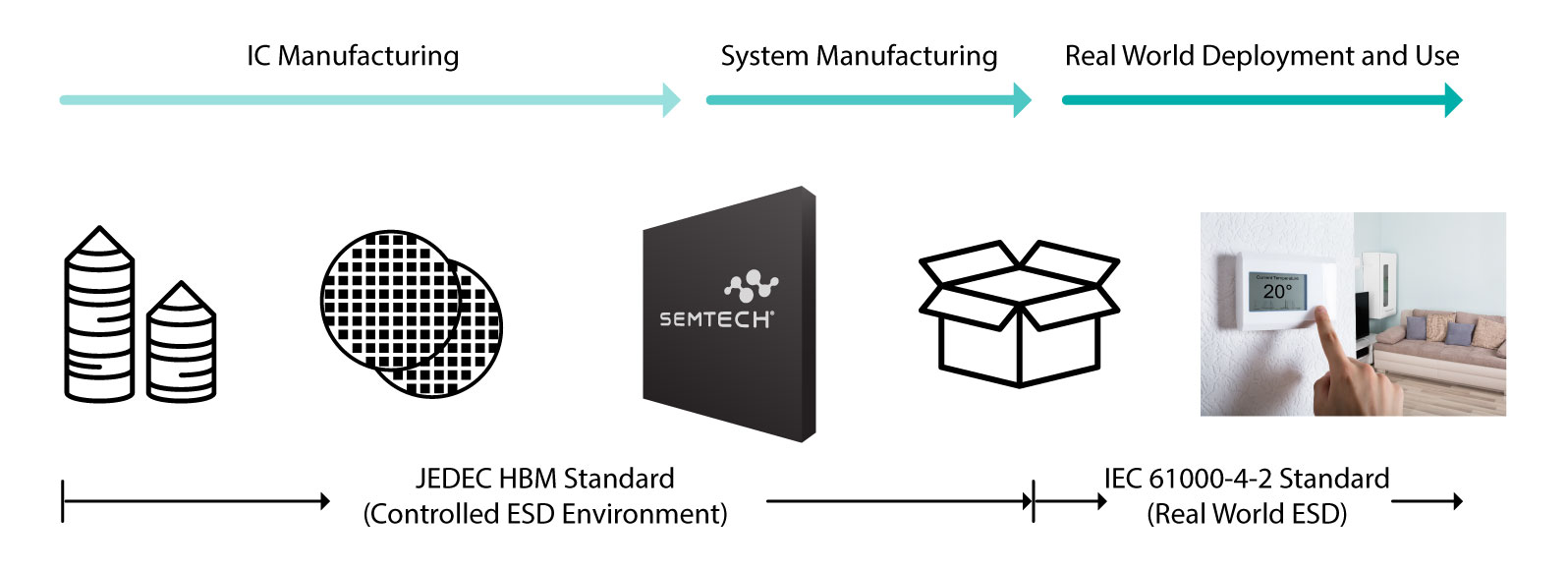
Any IC is vulnerable to ESD threats, even in a well-controlled, clean IC manufacturing environment. Processing, assembling, testing, and packaging are exposed to ESDs in any manufacturing step. The semiconductor industry uses different test models to simulate ESD events to determine the ESD robustness of a particular IC. Every IC needs to go through some level of ESD testing to prove it is fit for use. HBM is the most widely accepted ESD test to ensure the IC can survive the manufacturing process offering effective ESD control. It uses a test setup that simulates a scenario of a charged human body touching an IC and discharging the disastrous ESD through the IC to the ground. The human body is one of the most common generators of ESD, and the transfer of charge happens through physical contact only.
The HBM test involves discharging a capacitor through a resistor, which simulates ESD from a human body to an IC. The test voltage ranges from ±2kV to ±8kV. The HBM consists of a 100pF capacitor, charged to the desired test voltage and discharged through a 1500Ω resistor to the IC under test. This RC network creates a current source replicating a charged human body injected into the device under test. The device must survive the test without any damage. The test setup is shown in Figure 2. The current waveform for this test is shown in Figure 3. The rise time of the component level HBM current surge is 5-10ns, and the decay time is around 150ns.
.jpg?width=1160&height=443&name=Figure2%20(2).jpg)
Figure 2. Simulation circuit of component-level HBM.jpg?width=2385&height=926&name=Figure3%20(2).jpg) Figure 3. HBM current waveform
Figure 3. HBM current waveform
System-Level ESD Protection: IEC 61000-4-2 Standard
The IEC 61000-4-2 is a well-accepted international ESD testing standard using a human body model at system-level hardware. This system-level ESD standard, like HBM, also simulates a charged person discharging into an electronic system. But IEC 61000-4-2 standard is significantly more substantial than the component-level ESD defined by HBM. This system-level test aims to ensure that the device can survive transient events during different operating conditions in the hands of real-world applications' end users, including lightning protection. For this purpose, the released product must be tested against a rigorous ESD standard that simulates real-world transient conditions.
 The IEC 61000-4-2 test setup uses a 150pF capacitor charged to the specified voltage. It is then discharged into a component pin through a 330Ω resistor. The test setup is shown in Figure 4, and the ESD current waveform is shown in Figure 5. The rise time is swift, 0.7 to 1ns, with a second peak at 30ns and a total duration of only 60ns. Notice that a larger capacitance is discharged through a smaller resistor in the system-level IEC 61000-4-2 test setup (Figure 4) compared to the component-level HBM test (Figure 2) setup. This setup changes the current waveform’s rise time and peak current value.
.jpg?width=1129&height=413&name=Figure4%20(1).jpg) Figure 4. Simulation circuit of system-level IEC 61000-4-2
Figure 4. Simulation circuit of system-level IEC 61000-4-2
.jpg?width=1578&height=1406&name=Figure5%20(1).jpg) Figure 5. IEC 61000-4-2 current waveform
Figure 5. IEC 61000-4-2 current waveform
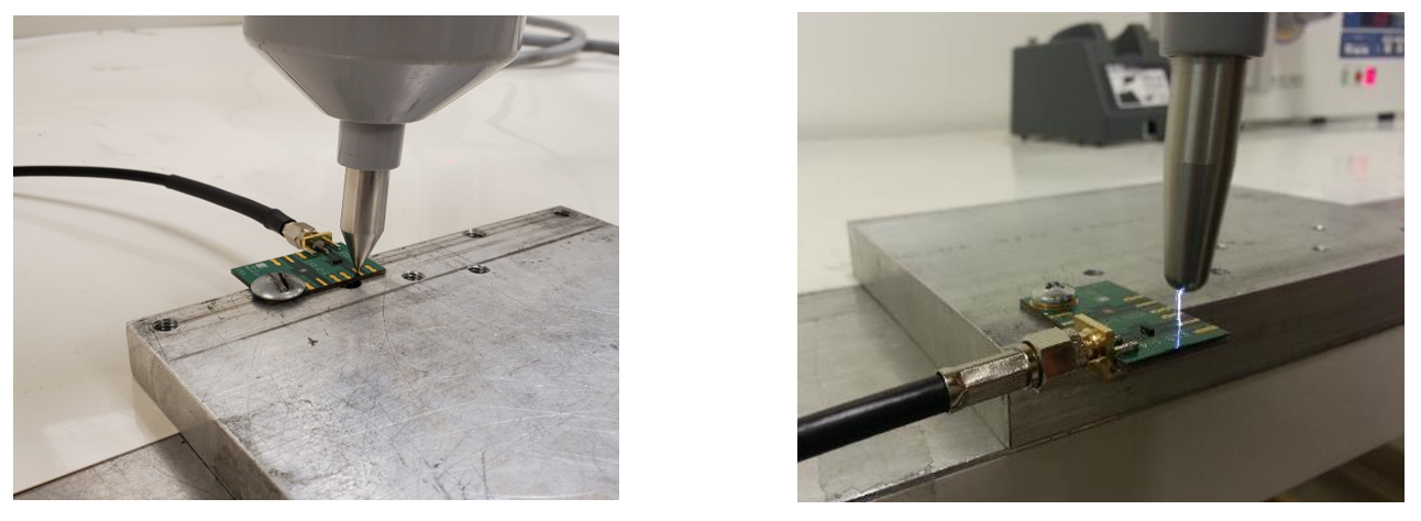
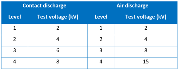
The IEC 61000-4-2 is divided into four standard levels (level 1 to level 4) depending on two different testing procedures – the contact and air discharge methods. The contact discharge method involves the ESD from the ESD test gun into the component through direct contact with the device under the test. The air discharge method is used for cases where contact discharge testing cannot be applied. In this case, the ESD test gun is brought closer without touching the component under the test. Figure 6 shows both the contact and air discharge methods.

Figure 6. Contact discharge method (left) and Air discharge method (right)
Table 1 lists the four levels and test voltages for contact and air discharge methods. The table shows that a level 4 contact discharge of 8kV equals a 15kV air discharge.
 Table 1. IEC 61000-4-2 test levels
Is ±2kV ESD Protection Enough for IoT Devices?
Now that we know the HBM and IEC 61000-4-2 testing models let us check the peak current level of ±2kV for both component and system-level testing. The peak current is a significant parameter for an IC to survive the ESD tests. Table 2 shows the peak current data comparison. It is noticeable in Table 2 that the peak current of a ±2kV HBM is 1.33A, and of a ±2kV system level is 7.5A. The peak current of a ±2kV HBM is 5.6 times lower than the pulse current of ±2kV IEC 61000-4-2. Table 2 also shows that the peak pulse current of ±8kV HBM testing (5.33A) is lower than the ±2kV IEC 61000-4-2 level testing (7.5A). That means, even if an IC passes the ±8kV component level HBM test, it may get damaged by a ±2kV system level IEC 61000-4-2 testing.
|
IEC Level (Contact discharge) |
Test voltage (kV) |
Component-level HBM Ipp (A) |
System-level IEC 61000-4-2 Ipp (A) |
| 1 | 2 | 1.33 | 7.5 |
| 2 | 4 | 2.67 | 15.0 |
| 3 | 6 | 4.00 | 22.5 |
| 4 | 8 | 5.33 | 30.0 |
Table 2. Peak current comparison
Figure 7 shows the waveform comparison of the two peak currents at ±8kV test voltage. It is visible from this diagram that the first peak for IEC 61000-4-2 happens in less than 1ns of rise time with a very high peak current. The highest peak for the HBM occurs around 5-10ns, and the peak current is much less than the IEC 61000-4-2. Even the second peak current is around 18A, which is way more than the peak of the HBM. Overall, the energy carried by the IEC 61000-4-2 is much higher than that of an HBM curve. A faster and more robust ESD protection is required to shield any electric circuit from system-level ESD.
.jpg?width=811&height=578&name=Figure7%20(1).jpg) Figure 7. Comparison of peak pulse current between HBM and IEC 61000-4-2
Figure 7. Comparison of peak pulse current between HBM and IEC 61000-4-2
The number of strikes is another essential thing to consider. One positive and one negative strike is performed in the component level HBM, whereas IEC 61000-4-2 requires a minimum of ten positive and ten negative strikes for the IC to survive. An IC can survive one single ESD strike but may get damaged in any repetitive ESD strike. Is ±2kV ESD protection enough? The most straightforward answer is that the design or systems engineers should consider the system-level IEC 61000-4-2 standard to determine if the IC will endure the ESD event. ±2kV component level HBM is good for the manufacturing environment. But the system-level IEC 61000-4-2 testing is necessary for an IC to survive in the end-user environment, specifically in IoT applications where the sensors and devices may reside outdoors or in harsh industrial environments.
Implementing ESD Protection in IoT Devices: Transient Voltage Suppressor (TVS) Diodes and More
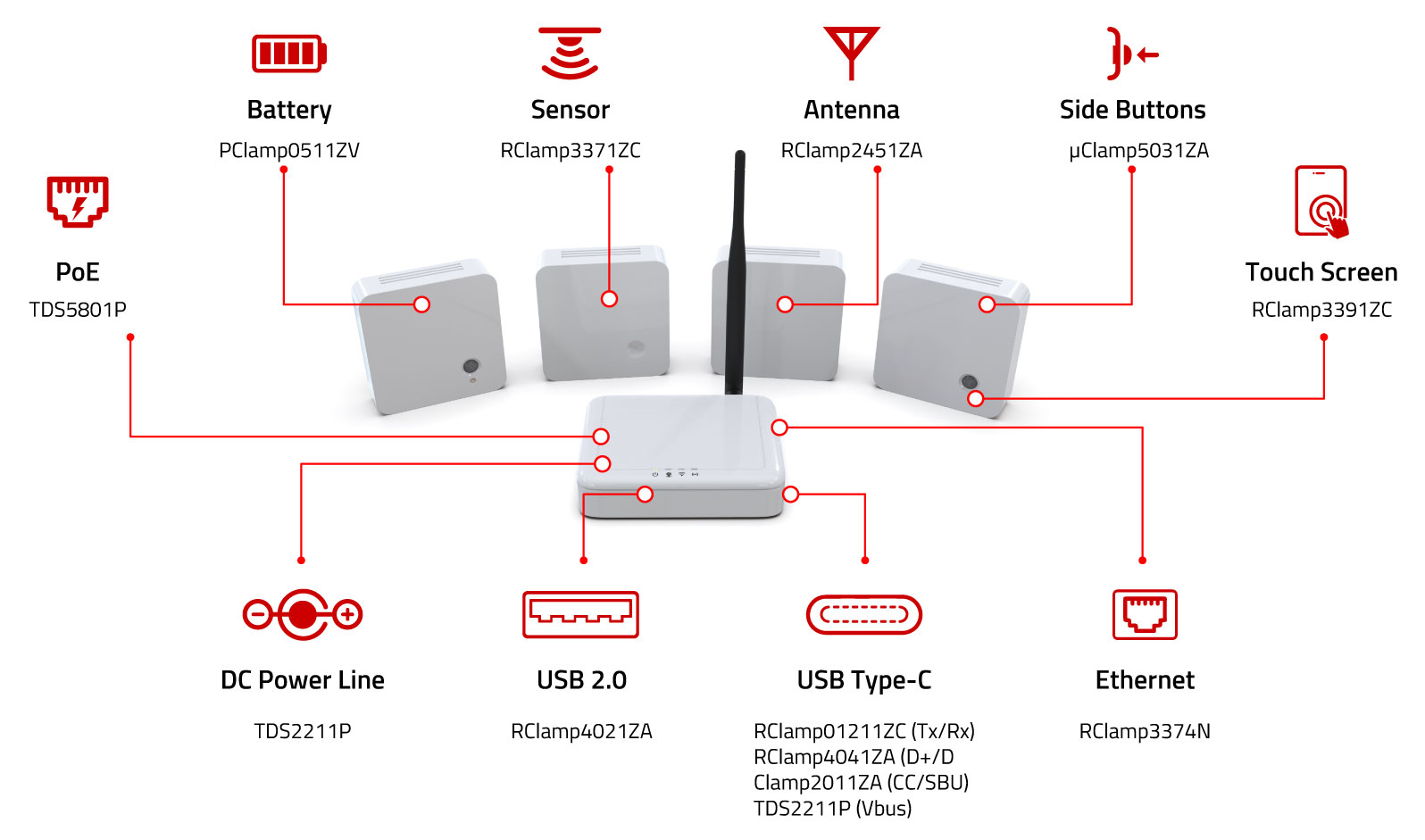
The previous discussions show what type of ESD or circuit protection devices are required for an IoT device. Now let us also review how to provide sufficient protection to the IoT ports and interfaces from electrical overstress (EOS) events. ESD protection can be achieved by placing transient voltage suppressor (TVS) diodes on the data or power lines to protect the interface during the fast rise time transient events. Transient events can damage the IoT sensors and devices if not appropriately safeguarded. The TVS diodes protect data ports from ESD threats by arresting the system level ESD peak in less than a nanosecond, diverting high currents from the data port. Under normal operating conditions, the TVS diode presents a high-impedance path to the circuit, making the device appear open. It does not interfere with the signal transfer. Table 3 lists ESD protection devices to shield the ports and interfaces of IoT gateways, sensors, servers, and other devices from electrical transients, EOS, and ESD events (Figure 8).
| Interface to Protect | Part Numbers | # of Lines | Configuration | VRWM | ESD Rating Contact/Air | Surge Rating (8/20µs) | Clamping Voltage (8/20µs) | Cap (Max) | Package Dimensions |
| Antenna | RClamp®2451ZA | 1 | Bidirectional | 24V | ±14kV/±18kV | 4A | 5.5V | 0.45pF | DFN (0.6x0.3x0.25mm) |
| Sensors | RClamp3371ZC | 1 | Bidirectional | 3.3V | ±10kV/±17kV | 9A | 5.4V | 0.25pF | DFN (0.6x0.3x0.25mm) |
| Ethernet | RClamp3374N | 4 | Bidirectional | 3.3V | ±30kV/±30kV | 40A | 25V | 5pF | DFN (3.0x2.0x0.6mm) |
| USB-C | RClamp01211ZC (Tx/Rx) | 1 | Bidirectional | 1.2V | ±10kV (Contact) | 2.5A | 10.3V (0.2/100ns) | 0.2pF | DFN (0.6x0.3x0.25mm) |
| USB-C | RClamp4041ZA (D+/D-) | 1 | Bidirectional | 4.0V | ±30kV/±30kV | 20A | 5.6V | 0.65pF | DFN (0.6x0.3x0.25mm) |
| USB-C | µClamp®2011ZA (CC/SBU) | 1 | Bidirectional | 20V | ±22kV/±30kV | 3A | 33.8V | 13pF | DFN (0.6x0.3x0.25mm) |
| USB-C | TDS2211P (VBus) | 1 | Unidirectional | 22V | ±30kV/±30kV | 40A | 27.6V | 175pF Typical | DFN (1.6x1.6x0.55mm) |
| USB 2.0 | RClamp4021ZA | 1 | Bidirectional | 4.0V | ±20kV/±25kV | 6V | 0.55pF | DFN (0.6x0.3x0.25mm) | |
| Touch Screen | RClamp3391ZC | 1 | Bidirectional | 3.3V | ±8kV/±15kV | 7A | 5V | 0.20pF | DFN (0.6x0.3x0.25mm) |
| Side Buttons | µClamp5031ZA | 1 | Bidirectional | 5V | ±30kV/±30kV | 7.5A | 7.6V | 13pF | DFN (0.6x0.3x0.25mm) |
| Battery | PClamp®0511ZV | 1 | Bidirectional | 5V | ±30kV/±30kV | 115A | 9V | 275pF | DFN (1.0x0.6x0.25mm) |
| DC Power Line | TDS2211P | 1 | Unidirectional | 22V | ±30kV/±30kV | 40A | 28V | 175pF | DFN (1.6x1.6x0.55mm) |
| PoE | TDS5801P | 1 | Unidirectional | 58V | ±15kV/±20kV | 20A | 70.2V | 72.8pF | DFN (1.6x1.6x0.55mm) |
Table 3. ESD protection devices of IoT devices per interface and port

Figure 8. ESD protection of IoT devices
Securing the Future of IoT: Circuit Protection Devices and ESD Protection
IoT devices and applications significantly improve our quality of life. It improves productivity, reduces human labor, and improves work safety in industrial and manufacturing applications. According to Fortune Business Insights, the global IoT market size is projected to grow from $662.21 billion in 2023 to $3352.97 billion in 2030 at a CAGR of 26.1%. With the massive popularity of IoT, it is critical to adequately protect each IoT interface, data, and communication port from ESD threats with elements like transient voltage suppression diodes. Semtech is a leading manufacturer of highly efficient and trusted ESD protection products. Contact Semtech while designing your next IoT device or application and protect it from all possible ESD and EOS events.
Semtech®, the Semtech logo, PClamp®, RClamp®, and µClamp® are registered trademarks or service marks of Semtech Corporation or its affiliates. Other product or service names mentioned herein may be the trademarks of their respective owners.
