Reducing Clamping Voltage
In part one, we learned transient voltage suppressor (TVS) clamping voltage is a key protection parameter. TVS manufacturers are constantly working to lower clamping voltage to keep up with ever shrinking IC geometries and increased sensitivity to overvoltage events. One method to achieve lower clamping is to engineer the device to “snapback” to a lower voltage once triggered. The snapback can be shallow, or deep depending on the intended application. One method of achieving a deep snapback is to design a self-triggering thyristor TVS structure (Figure 4).

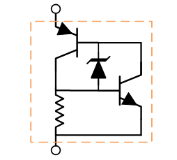 Figure 4 – Deep Snapback TVS Structure © Semtech Corporation
Self-triggering is achieved by causing the collector-base of the PNP transistor to breakdown at a specific voltage, which can be accurately controlled with a TVS structure. During a transient event, the TVS starts to conduct and current flows into the base of the NPN transistor. This in turn drives current into the base of the PNP transistor and so on until both transistors are driven into saturation. This causes the voltage between the two terminals to snapback or fall to a low level. Once the transient subsides, the device will return to a high impedance state as long as the voltage on the protected line is removed. One disadvantage of this type of protection solution is that “latch up” can occur in some applications. Latch up occurs when a TVS is triggered by a transient voltage event and remains conducting after the transient has dissipated. While deep snapback devices provide some of the lowest clamping voltage solutions available, latch up considerations may necessitate the use of a non-snapback or a shallow snapback device. A typical shallow snapback TVS circuit is shown in Figure 5.
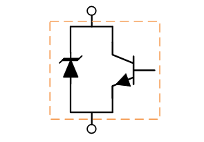 Figure 5 – Shallow Snapback Structure © Semtech Corporation
Here, the TVS is in parallel with the collector-emitter of a transistor with a floating base. The base is designed in such a way that once the TVS starts to conduct, the voltage across the collector-emitter terminals of the transistor will force the base to “punch-through.” The result is a slight or “shallow” snapback characteristic. A comparison of TVS IV characteristic curves is shown in Figure 6.
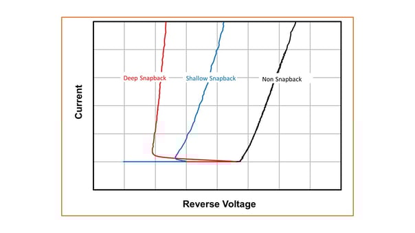 Figure 6 – TVS IV Characteristics © Semtech Corporation
Lowering the Capacitance
A TVS has to provide protection against transient events without affecting the normal operation of the circuit. This can be a challenge because parameters are often working against each other. For example, a TVS used on a high speed circuit has to present a low capacitance to avoid signal degradation. However, a device’s ability to absorb energy is related to the junction size. The larger the junction, the more energy it can absorb. The downside is that as junction size increases, the device capacitance also increases. A common way to reduce the effective capacitance is to use a low capacitance steering diode circuit in conjunction with the TVS (Figure 7).
 Figure 7 – Low Capacitance TVS © Semtech Corporation
The capacitance of the TVS is effectively “hidden” from the circuit. The design of the compensation circuit requires diodes with sufficient area to conduct transient current under forward bias conditions, and a reverse breakdown voltage greater than the breakdown voltage of the TVS. The resulting TVS is usually a monolithic device. Emerging standards such as USB4 and Thunderbolt 3 have strict insertion loss allocations for ESD protection. Semtech’s RailClamp® series devices rely on the aforementioned low capacitance structure to provide high levels of ESD protection on high-speed lines while meeting critical insertion loss requirements.

Packaging for Efficiency
Packaging is an important component in TVS construction. Most “diodes” utilize a wire bond structure to connect the die to the lead. The wire bond adds inductance and adds to the peak clamping voltage. Recall that V = L di/dt. For an 8kV ESD pulse, 1nH of inductance can add 30V to the peak clamping (V = 1nh 30A/ns). Many TVS devices still utilize wire bond structures, but higher performance devices minimize the series inductance by eliminating the wire bond. For example, Semtech’s Z-Pak™ series are chip scale devices with a proprietary epoxy coating. This structure provides the absolute minimum inductance without sacrificing structural integrity like traditional, uncoated chip scale packages. Multi-line devices are available that utilize chip-on-lead technology to eliminate wire bonds and minimize inductance.
Emerging standards, decreased on-chip protection and shrinking IC geometries are driving TVS device research and development. Modern TVS components are not “just diodes,” but intricate structures designed to protect today’s increasingly sensitive devices. Proper device selection requires careful consideration of circuit parameters.
Semtech has been a pioneer in TVS diode development for over 30 years. We have a diverse portfolio of devices for protecting legacy and next generation ports.

Semtech, the Semtech logo and RailClamp are registered trademarks or service marks, and Z-Pak is a trademark or service mark, of Semtech Corporation or its affiliates.